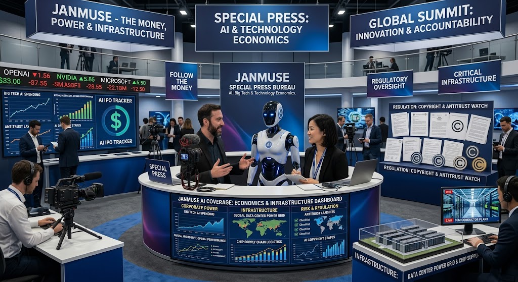
These Are the Cathedrals of the Artificial Intelligence Age
Across the globe, the landscape of infrastructure is undergoing a radical, silent transformation. In vast, nondescript industrial parks from the high deserts of the American West to the humid corridors of Southeast Asia, colossal data centers are rising at an unprecedented pace. These are the cathedrals of the artificial intelligence age—sprawling complexes designed to house tens of thousands of high-performance servers, each demanding an insatiable supply of power and space. These buildings represent billions of dollars in capital investment, fueled by a singular, urgent mission: to train the next generation of large language models. However, to the casual observer, these steel-and-concrete shells mask a deeper, more volatile reality.
While the media fixates on the rapid iteration of code and the competitive posturing of software CEOs, the true engine of this revolution is not found in lines of programming. It is found on the microscopic assembly lines of the most complex manufacturing facilities ever devised by man, where the race to build the hardware infrastructure is currently hitting a formidable, physical wall. There is a profound disconnect between the ethereal promise of AI software and the gritty reality of silicon fabrication. On Wall Street, the narrative is one of infinite scalability; if you throw enough capital at an algorithm, intelligence will follow.
Yet, beneath this veneer of digital ease lies the sobering truth of material science. The speed at which AI models evolve is not determined solely by the ingenuity of researchers, but by the physical throughput of semiconductor plants. We are currently witnessing a global bottleneck where the software ambitions of trillion-dollar tech giants collide with the rigid, unforgiving realities of manufacturing physics. While investors focus on quarterly revenue growth and software feature sets, the real limiting factor is the lead time on hardware production.
The industry is realizing that chips are not just commodities you can order in bulk; they are the result of an intricate, multi-stage dance of chemistry and precision engineering. The hype cycle of AI has far outpaced our ability to physically manifest the silicon required to sustain it. To understand the bottleneck, one must look at a process that has become the industry’s most critical constraint: CoWoS, or Chip-on-Wafer-on-Substrate. Imagine a standard processor as a lone worker in a factory.
As AI Workloads Grew More Complex, Traditional Single-chip Designs Hit a Ceiling
As AI workloads grew more complex, traditional single-chip designs hit a ceiling—they simply couldn’t move data fast enough or manage the heat generated by massive computations. CoWoS solves this by acting as a sophisticated architectural hub. In this process, the main AI processor is placed onto an interposer—a microscopic silicon highway—alongside other high-performance components. These elements are not just resting next to each other; they are fused together in a vertical stack. By placing the components on the same base, the distance data has to travel is reduced to mere micrometers, drastically lowering energy consumption and latency.
It is a masterpiece of precision engineering that allows multiple chips to communicate as if they were a single, unified entity, providing the immense bandwidth required to train modern AI models. At the heart of the CoWoS package lies another revolutionary component: High Bandwidth Memory, or HBM. Without this, even the most powerful AI chip would be trapped in a state of idle waiting, starved of the vast quantities of data it needs to process. HBM involves stacking layers of memory chips directly on top of one another, like a skyscraper of data storage.
When these memory stacks are integrated into the CoWoS package, they act as an immediate, lightning-fast reservoir for the processor. The challenge, however, is that this integration process is exponentially more difficult than standard manufacturing. You are not just fabricating a chip; you are managing the assembly of highly sensitive, high-value components that must function perfectly in unison. If one part of the stack fails, the entire package—costing tens of thousands of dollars—is rendered useless. This delicate, high-stakes integration is precisely where the global AI supply chain slows to a crawl, creating a physical scarcity that no amount of software investment can bypass.
This scarcity has turned TSMC into the most vital choke point in the global economy. Because the process is so specialized, the availability of CoWoS capacity has become the ultimate dictator of the AI industry’s delivery schedules. When Nvidia announces its latest flagship GPU, it is not merely announcing a product; it is announcing a product that must wait in a massive, months-long queue at TSMC’s packaging facilities. The manufacturing capacity is not just a secondary concern; it is the primary heartbeat of the company’s roadmap. If TSMC cannot package the chips, the chips cannot be shipped, and the entire AI ecosystem stalls.
This reality has created a scenario where hyperscalers like Microsoft, Amazon, and Meta are not just buying hardware; they are effectively competing for a limited, guarded slice of TSMC’s production schedule.
Every Delay in the Expansion of CoWoS Capacity Ripples Outward
Every delay in the expansion of CoWoS capacity ripples outward, delaying data center rollouts, stalling AI model training, and shifting the projected timeline of profitability for the entire tech sector. The financial stakes for companies like Microsoft, Meta, and Google are staggering. These firms are pouring billions of dollars into massive data center projects, counting on a steady stream of specialized silicon to justify their astronomical capital expenditures. When those expected chips are delayed by packaging constraints, these companies face a high-risk scenario where massive, completed data centers sit empty—or under-utilized—costing millions in overhead while failing to generate the expected intelligence output.
It is a game of high-stakes gambling where the chips on the table are literal silicon. For these corporations, the inability to get their hardware on time leads to missed strategic windows, damaged market sentiment, and the potential for a significant cooling in investor enthusiasm for AI. The volatility of their stock price is now, in many ways, tethered to the efficiency of a single, highly specialized production process occurring inside a few cleanrooms in Taiwan, making the economics of the AI era fragile and dangerously concentrated. Stepping into a modern semiconductor cleanroom is like entering a temple of silence and precision.
The air is filtered thousands of times an hour to remove a single speck of dust, which, at this scale, would act like a boulder crashing into a city. In these sterile, white-lit environments, workers use robotic arms to perform operations that push the very boundaries of physics. Stacking chips within a CoWoS package requires alignment down to the nanometer. A variation in temperature or a microscopic shift during the bonding process can result in a catastrophic failure. The workers here are not merely assembling parts; they are orchestrating a process that requires absolute stability and perfection.
It is a grueling, high-pressure environment where the slightest human error or environmental fluctuation can sabotage weeks of work. This is the frontline of the technological cold war, a place where the grandeur of AI’s future is defined by the absolute perfection required in the present. The difficulty of scaling CoWoS lies in its fundamental complexity compared to traditional chip fabrication. Standard chip-making relies on massive, repeatable lithography processes that can be automated and ramped up relatively easily once the lines are set. Packaging, however, is inherently more variable and time-consuming.
Because it involves stacking, bonding, and testing multiple heterogeneous components, it cannot simply be accelerated by throwing more capital at the problem overnight. It requires the construction of entirely new, state-of-the-art packaging facilities that take years to bring online.
We Are Seeing the Limits of Industrial Scaling in Real Time
This is why, despite the massive surge in demand for AI, capacity is projected to only double by 2028. We are seeing the limits of industrial scaling in real time. Unlike software, which can be duplicated infinitely with a click, hardware manufacturing is bound by the slow, painful process of building the physical capacity to create. The bottleneck is not just a hurdle; it is a profound realization of the friction that exists between digital aspiration and physical reality. Behind the closed doors of boardrooms in Silicon Valley, a quiet, desperate scramble is unfolding.
Tech giants—the titans of the cloud and the masters of generative AI—are no longer just competing on software code or model architecture. Instead, they are engaged in a high-stakes lobbying war for guaranteed priority in TSMC’s production queue. It is a modern-day gold rush where the resource in question isn’t land or minerals, but space on an advanced packaging line. To secure a place in the CoWoS manufacturing pipeline is to secure the ability to compete in the next decade of AI development. These companies arrive at the negotiating table with deep pockets and aggressive delivery schedules, hoping to nudge their orders to the front of the line.
But TSMC, as the sole gatekeeper of the industry’s most critical fabrication step, holds all the leverage. Every slot on a CoWoS line is a bottlenecked asset, and for those who lose the race for priority, the consequences are immediate: stalled server deployments, missed product launches, and potentially billions of dollars in lost market capitalization as their AI ambitions grind to a halt. To understand the gravity of the situation, one must look at the backlog of orders currently trapped in the pipeline. Imagine a massive, intricate gridlock where high-performance compute dies sit idle, waiting for the final stage of assembly that will turn them into usable chips.
This is not a failure of design; it is a fundamental mismatch between the explosion of AI demand and the glacial speed of physical facility deployment. The backlog represents millions of individual GPU units currently relegated to a state of stasis. Every week, the queues grow longer, fueled by the relentless hunger of hyperscalers for more compute power.
This Visual Backlog Is the Physical Embodiment of the Industry’s Greatest Fear
This visual backlog is the physical embodiment of the industry’s greatest fear: the inability to scale despite having the capital and the intent to do so. For investors and analysts watching the industry, this backlog is the most critical metric of all. It tells the story of an industry hitting a hard physical wall, where even the most aggressive financial projections must be revised downward because the chips simply cannot be finished fast enough to meet the demand of the global market. The reality of this constraint is now reflected in the concrete strategic moves made by Taiwan Semiconductor Manufacturing Company.
The firm has officially committed to a massive, multi-year expansion, with the goal of doubling its current CoWoS capacity by the year 2028. This is not merely an incremental upgrade; it is an industrial mobilization on a global scale. Evidence from the latest industry reports confirms that this target is the cornerstone of TSMC’s roadmap, designed to alleviate the crushing pressure applied by hyperscalers. Achieving this, however, is a monumental task. Doubling capacity requires the construction of new fabrication plants—or ‘fabs’—that are specifically engineered for the delicate, high-precision task of CoWoS.
These facilities must be equipped with the latest bonding and testing technology, requiring thousands of man-hours to calibrate and stabilize. The commitment to 2028 acts as a definitive beacon for the industry, setting a clear, albeit challenging, horizon for when the current acute shortage might finally begin to ease into a more manageable state of supply and demand. The capital expenditure, or CapEx, associated with this expansion is staggering. Doubling CoWoS capacity requires billions of dollars in upfront investment before a single saleable chip is produced.
We are talking about the construction of highly specialized cleanrooms, the acquisition of advanced lithography and bonding machinery, and the massive energy and logistical costs involved in maintaining a world-class manufacturing environment. For TSMC, this represents a massive risk, as they must balance the current urgent demand against the long-term potential for market saturation. Investors are closely scrutinizing these expenditures, as they fundamentally alter the company’s financial profile. This is not just a technological investment; it is a massive bet on the sustained growth of the AI hardware ecosystem.
The sheer scale of the CapEx required also serves as a deterrent to potential competitors, creating a high barrier to entry that keeps the CoWoS market concentrated. As billions flow into these new facilities, the financial pressure to ensure high yields and consistent output becomes the dominant concern for the company’s leadership and its primary stakeholders.
In Response to These Constraints, We Are Witnessing a Transformation in Chip Architecture
In response to these constraints, we are witnessing a transformation in chip architecture. Companies like Google and Amazon have shifted their strategies, moving away from relying solely on third-party silicon providers. Instead, they are pouring resources into developing their own custom ASICs—Application-Specific Integrated Circuits. These custom chips are optimized for the specific workloads of their data centers, offering higher efficiency and better performance per watt than off-the-shelf solutions. However, even these custom designs are not immune to the packaging bottleneck. These proprietary ASICs still rely on the exact same CoWoS fabrication processes at TSMC.
The custom-silicon movement was intended to bypass the supply constraints and high costs of standard GPUs, but it has ultimately found itself at the mercy of the same manufacturing wall. By designing their own chips, these firms are essentially competing with the very manufacturers they rely on, fighting for the same limited packaging slots that define the entire sector’s production output. Does proprietary chip design actually help circumvent the packaging bottleneck? The short answer is no, and in some cases, it may even exacerbate the challenge. While a custom design can be more efficient, it often requires equally sophisticated and complex packaging solutions to reach its full potential.
By diversifying the types of chips that require CoWoS, hyperscalers are actually increasing the diversity of the tasks that TSMC must manage within its already strained facilities. Design innovation is effectively outpacing manufacturing capacity. Every new, faster, or more efficient chip that comes out of an R&D lab is another line item on a production schedule that is already full for years. Proprietary design allows for custom tuning of hardware performance, but it provides no shortcut around the physical realities of the assembly line. The bottleneck is agnostic to design complexity; it cares only about the volume and the intricate physical stacking process.
As long as the physical packaging capacity remains fixed, the brilliance of custom chip design will remain tethered to the physical limitations of the fabrication house. This leads us to the broader geopolitical reality of the situation: the extraordinary concentration of advanced packaging technology within the borders of Taiwan. The global AI industry is effectively hanging on the stability of a single, highly specialized supply chain ecosystem. While the design of these chips may happen in offices across the United States, the physical ‘birth’ of the final product occurs in Taiwanese facilities that are unparalleled in the world.
This concentration is the result of decades of investment, talent accumulation, and institutional knowledge. It is a sophisticated, deeply integrated web of suppliers and experts that cannot be replicated easily or quickly.
The Geopolitical Risk Here Is Significant
The geopolitical risk here is significant, as the entire trajectory of the global AI race is tied to the operational continuity of these specific industrial clusters. Any disruption, whether from geopolitical tension or environmental events, would have a catastrophic ripple effect, grounding the AI industry’s hardware growth and creating a bottleneck that no amount of software innovation could possibly overcome. The United States and other regions are attempting to build domestic packaging capacity, but they face a monumental task.
The difficulty of replicating the Taiwan ecosystem is not just about building buildings or buying machines; it is about replicating the entire infrastructure of specialized labor, deep-rooted supply chains, and decades of manufacturing experience. We have seen significant capital injected into domestic fabrication efforts, but the reality remains that scaling up a new, world-class packaging center takes years of trial and error. The ‘Taiwan model’ is a product of an iterative, highly collaborative environment that is remarkably difficult to transport. Even with government incentives and massive corporate backing, domestic efforts remain in their infancy compared to the mature production lines across the Pacific.
As these new centers slowly come online, the industry is forced to continue its reliance on the existing Taiwanese nodes. It is a slow, grueling process of building industrial history from scratch, highlighting once again that in the world of high-end hardware, location and established expertise are the ultimate drivers of progress. The fragility of the AI supply chain is hidden within the microscopic margins of error in CoWoS packaging. When TSMC binds high-bandwidth memory to a central compute die, the tolerances are sub-micron. If a single connection fails during this complex, multi-stage interposer process, the entire high-value GPU package is rendered worthless.
These yield rates are the silent tax on every dollar of capital expenditure spent by hyperscalers. A 90% yield isn’t just a 10% loss in volume; it represents millions of dollars in sunken R&D, specialized substrate material, and precious machine time vanished in a millisecond of thermal expansion. Manufacturers are essentially playing a high-stakes game of physics, where the cost of a failed unit rises exponentially with the complexity of the chip. As we push toward more dense configurations, the economic threshold for acceptable failure becomes razor-thin.
It Forces Companies to Weigh the Costs of Aggressive
It forces companies to weigh the costs of aggressive, innovative packaging against the reality of mass-production entropy, making the factory floor the ultimate arbiter of which AI models actually get to train on the latest silicon. Every percentage point lost to packaging yield directly echoes through the global economy, manifesting as an artificial ceiling on GPU availability. Because these chips are not mass-produced like generic memory or basic controllers, the supply chain is hyper-sensitive to any bottleneck in the back-end assembly. When yield rates fluctuate, the reverberations are felt by every major technology firm, forcing them to pivot their deployment strategies based on the output of specific cleanrooms in Hsinchu.
It is a paradox of our age: the software is written in a global, distributed cloud, but the physical reality of the hardware is chained to the success rate of a single manufacturing process. If the packaging lines aren’t delivering, the GPUs aren’t shipping. This creates a precarious dependency where global AI progress is tied to the statistical probability of a successful bond. The industry isn’t just fighting for market share; it is fighting for the physical throughput of these specialized lines, knowing that any shortfall in packaging is an immediate constraint on the capacity of the world’s most advanced data centers.
The industry is acutely aware that the current CoWoS paradigm, while revolutionary, is not the final frontier. Engineers are now racing toward a transition to 3D IC packaging and complex chiplet architectures, which aim to decouple the compute logic from auxiliary components. By stacking logic die directly on top of each other, designers hope to bypass the physical space limitations of the horizontal interposer, effectively shortening the distance electricity travels and reducing heat. However, moving to these 3D stacks introduces a new nightmare of vertical thermal management and structural stress. Every transition away from the ‘tried and true’ CoWoS method introduces new vectors for systemic failure.
While the vision of a modular, stacked architecture promises a future where chips can be mixed and matched like building blocks, the reality of high-volume manufacturing remains elusive. For now, these designs are aspirational, awaiting the day when packaging technology can reliably sustain these vertical geometries without compromising the long-term integrity of the silicon. Transitioning from our current, refined CoWoS processes to next-generation stacking is not a simple matter of swapping software modules or upgrading a single piece of lithography equipment. It requires an entirely new ecosystem of assembly robotics, testing procedures, and specialized materials.
This transition period is measured not in months, but in multi-year cycles of calibration and qualification.
The Existing Infrastructure Is Optimized for 2
The existing infrastructure is optimized for 2. 5D, and pivoting to 3D requires us to effectively re-learn how to build hardware on an atomic level. During this shift, the industry risks a temporary plateau in performance gains as we struggle to move from the known, reliable paths to the uncertain terrain of true vertical integration. Hyperscalers and manufacturers are currently caught in this bridge-building phase, trying to maintain the output of today’s chips while pouring billions into the development of a, currently, unscalable future. It is a slow, methodical migration that acts as a silent brake on the aggressive timelines touted in boardrooms across the globe.
Looking back at the trajectory of the last decade, the fundamental truth becomes clear: we have been misled into believing that the chip design is the primary mover of innovation. In reality, the physical constraint of the manufacturing floor dictates the limits of our computational reality. Even the most elegant architecture remains a mere blueprint until it can be successfully packaged at scale. The bottleneck is not in the mind of the architect, but in the precision of the pick-and-place robotics and the purity of the chemical deposition processes. We are witnessing the end of an era where design could outpace fabrication. Today, the design is subservient to the packaging.
The hyperscalers are essentially ‘designing for the factory,’ tailoring their massive chips to fit within the limitations of what TSMC can successfully assemble. When we evaluate the future of AI, we must look not at the clock speed or the transistor count, but at the capacity and the throughput of the packaging lines. Fabrication is the bottleneck that defines the modern economy. As we gaze toward 2028, the doubling of TSMC’s CoWoS capacity represents more than just a statistical increase in volume; it marks a stabilization of the entire AI hardware market.
Success by 2028 will not be defined by the emergence of a magic new chip, but by the maturity and scale of the packaging infrastructure that brings these architectures to life. If the industry successfully navigates this expansion, we will see a shift from a supply-constrained environment to one where the focus returns to software efficiency and application deployment. The goal is to reach a state of industrial equilibrium, where the capacity to package advanced chips matches the insatiable demand of the world’s data centers. While the road ahead is paved with physical risks and material limitations, the industry’s commitment to doubling its capacity serves as a roadmap for progress.
By 2028, the true measure of technological dominance will be found in these specialized assembly lines, cementing manufacturing leadership as the ultimate strategic asset in the digital age.